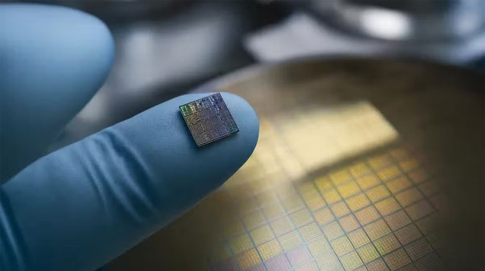
IBM has introduced what it describes as the world’s first chip technology below 1 nanometer. The IBM sub 1nm chip represents a watershed moment in semiconductor innovation. The technology can fit nearly 100 billion transistors onto a die roughly the size of a fingernail. This advancement nearly doubles the transistor density of IBM’s experimental 2nm chip, which engineers first demonstrated in 2021.
The smallest and most advanced chips currently contain around 80 billion transistors. Therefore, IBM’s breakthrough represents a significant leap forward. Moreover, the density improvement opens new possibilities for processing power and energy efficiency across multiple applications.
NanoStack Design
The technology is based on NanoStack, a three-dimensional transistor architecture that stacks and staggers complementary metal-oxide-semiconductor devices vertically along the z-axis. IBM previously developed the nanosheet transistor designs that major chip manufacturers now adopt at the 3nm and 2nm process nodes. However, NanoStack goes further by joining two nanosheet transistors into one vertical structure.
IBM can optimize each transistor layer independently and connect the two devices from opposite sides. Each transistor in the demonstrated structure contains three nanosheets measuring less than 5nm in thickness, roughly equivalent to 15 silicon atoms across. Additionally, spacers measuring about 9nm separate the nanosheets. IBM then bonds two of these transistor devices vertically using an extremely thin dielectric process. The company describes this bonding as one of the technology’s main innovations.

Different Materials
The upper and lower transistors can use different channel materials, metals, and dielectric materials. IBM therefore describes NanoStack as a transistor platform rather than a single manufacturing technique. The company believes it can continue developing the design through several generations, including 7 angstrom, 5 angstrom, 3 angstrom, and potentially 1 angstrom technologies.
One angstrom equals one ten-billionth of a meter, while 10 angstroms equal one nanometer. Jay Gambetta, director of IBM Research and an IBM Fellow, said the company was not simply reducing transistor sizes. Instead, IBM is changing how chips are built to improve performance and energy efficiency.
Performance Gains
IBM’s internal comparisons with its 2nm technology show that the IBM sub 1nm chip could provide up to 50 percent higher performance while consuming the same amount of power. Alternatively, it could reduce power consumption by as much as 70 percent while delivering the same level of performance. Huiming Bu, IBM’s vice president of silicon technology research and development, similarly said the technology could improve performance by 50 percent compared with the best chips currently available. Moreover, it could reduce power use by 70 percent.
Improved Memory Density
IBM also reported a 40 percent improvement in the scaling of static random-access memory cell area compared with its 2nm technology. The company describes the improvement as a step the semiconductor industry has not achieved in more than a decade. The increase could prove especially important for artificial intelligence accelerators, which rely heavily on on-chip memory capacity and bandwidth.
Greater SRAM density could allow chip designers to place larger caches and more on-die memory closer to processing units. This approach would reduce the amount of data that needs to move across the chip during AI training and inference tasks. Therefore, memory architecture efficiency improves considerably.
Three-Dimensional Scaling
Bu describes NanoStack as a new approach that moves chip scaling fully into three dimensions. He said the technology could give the semiconductor industry at least another decade of progress. Manufacturing will transition from nanometer-scale processes into the angstrom era. Instead of only making transistors smaller across a flat surface, this system increases density by arranging devices vertically.
Production Timeline
IBM believes the IBM sub 1nm chip could begin appearing in production applications within the next five years. The company expects the technology to eventually support processors, graphics chips, mobile system-on-chips, and SRAM memory arrays. So multiple product categories will ultimately benefit from this breakthrough. Finally, this advancement positions IBM as a leader in next-generation semiconductor design as the industry approaches fundamental physical limits.